Miniature systems based on additive processes
Wireless MEMS microphone system.
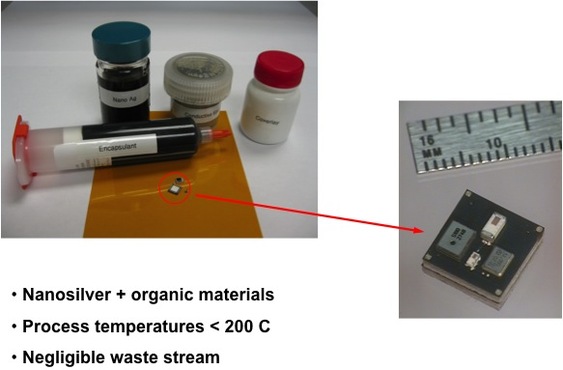
We have developed processes that combine the benefits of fine feature embedded conductors with the many advantages of embedded component packaging. Our technology brings together advanced adhesives, nanoparticle silver conductors and small surface-mount electronic components to produce miniature modular blocks active and passive devices. 3D configurations are achieved by stacking the miniature modules using vertical interconnects.
The wireless MEMS microphone system shown here has two layers of embedded components with the microphone and antenna exposed on the top surface.
Click for more information about our fine-feature conductors, available substrate materials, embedded component packaging, and module interconnection.
The wireless MEMS microphone system shown here has two layers of embedded components with the microphone and antenna exposed on the top surface.
Click for more information about our fine-feature conductors, available substrate materials, embedded component packaging, and module interconnection.